Semiconductor Heterojunction Lasers: Light Emission Devices Enabled by Bandgap Engineering
The development of semiconductor heterojunction lasers represents a pivotal advancement in optoelectronics, merging the principles of quantum mechanics with materials science to create highly efficient light-emitting devices. These lasers leverage carefully engineered heterostructures—interfaces between dissimilar semiconductors—to confine charge carriers and photons, enabling stimulated emission with remarkable precision. Unlike conventional homojunction lasers, heterojunction designs exploit abrupt changes in bandgap energy to form potential barriers that dramatically improve performance.
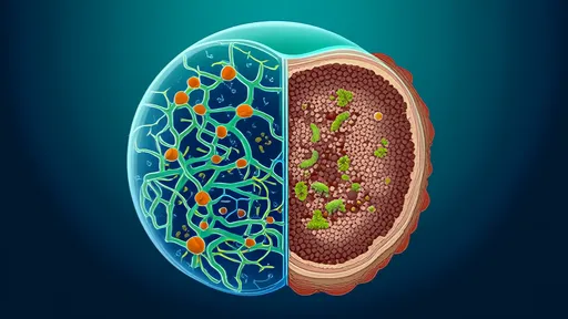
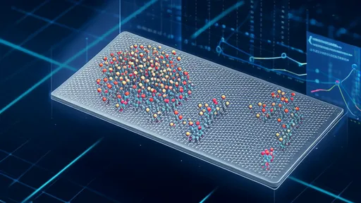
At the heart of heterojunction laser technology lies the strategic manipulation of energy bands. By epitaxially growing ultrathin layers of semiconductors with differing bandgaps (such as GaAs and AlGaAs), engineers create quantum wells where electrons and holes recombine with exceptional efficiency. The discontinuity in conduction and valence bands at these interfaces acts as a natural trap for both charge carriers and emitted photons, reducing threshold currents and enabling continuous-wave operation at room temperature—a feat that revolutionized laser diode practicality.
The journey toward modern heterojunction lasers began with the groundbreaking work on double-heterostructure designs in the 1960s. Early researchers discovered that sandwiching a narrow-bandgap material between two wider-bandgap layers produced an optical cavity that simultaneously confined injected carriers and guided light. This architectural breakthrough solved the critical challenge of carrier leakage that plagued earlier laser diodes, dropping threshold current densities from ~50,000 A/cm² to below 1,000 A/cm² practically overnight.
Material selection and lattice matching prove crucial in heterojunction laser fabrication. While III-V semiconductors like GaAs/InP systems dominated early developments, contemporary devices incorporate sophisticated quaternary alloys (InGaAsP) and strained-layer superlattices to access specific wavelength ranges. The emergence of nitride-based heterostructures (GaN/AlGaN) further expanded applications into the blue and ultraviolet spectrum, enabling white-light solid-state lighting and high-density optical storage solutions.
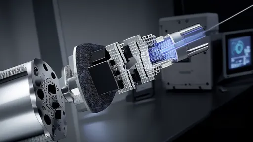
Modern heterojunction lasers showcase astonishing diversity in their implementations. Edge-emitting lasers employ carefully cleaved facets to form optical resonators, while vertical-cavity surface-emitting lasers (VCSELs) utilize distributed Bragg reflectors to achieve emission perpendicular to the wafer surface. Quantum cascade lasers take heterostructuring to extremes, with hundreds of precisely grown layers enabling mid-infrared emission through intersubband transitions rather than conventional bandgap recombination.
The impact of these engineered light sources permeates countless technologies. Fiber-optic communication systems rely on heterojunction lasers for converting electrical signals into coherent light pulses with minimal dispersion. Consumer electronics integrate them as precision light sources in Blu-ray players and laser printers. Industrial applications range from material processing to medical diagnostics, where the ability to tune emission wavelengths through bandgap engineering enables targeted tissue interaction.
Ongoing research pushes heterojunction laser capabilities into new frontiers. Nanoscale engineering creates photonic crystal lasers that manipulate light through periodic dielectric structures. Silicon photonics seeks to integrate III-V heterostructures with CMOS technology for optical interconnects in next-generation computing. Meanwhile, developments in two-dimensional material heterostructures (like graphene/MoS₂) hint at ultra-thin flexible laser devices that could transform wearable optoelectronics.
As bandgap engineering techniques grow more sophisticated—incorporating atomically precise deposition and strain-tuning methods—heterojunction lasers continue to break performance barriers. Their evolution stands as testament to how fundamental quantum mechanical principles, when creatively applied through materials science, can yield technologies that reshape entire industries. From the infrared beams carrying global internet traffic to the laser pointers illuminating lecture halls, these remarkable devices exemplify the transformative power of semiconductor heterostructures in harnessing light.
By /Jun 19, 2025

By /Jun 19, 2025

By /Jun 19, 2025

By /Jun 19, 2025
By /Jun 19, 2025

By /Jun 19, 2025

By /Jun 19, 2025

By /Jun 19, 2025

By /Jun 19, 2025

By /Jun 19, 2025
By /Jun 19, 2025

By /Jun 19, 2025

By /Jun 19, 2025

By /Jun 19, 2025

By /Jun 19, 2025

By /Jun 19, 2025

By /Jun 19, 2025